What’s SWD?
Serial Wire Debug (SWD) is a two-pin interface and protocol developed by ARM specifically for debugging and programming microcontrollers. It serves as a modern, space-saving alternative to traditional JTAG (Joint Test Action Group) interfaces, making it the standard debug method for ARM Cortex-M processors. Now why am I saying this to you and why does it matter? Well because I recently got into the world of vape hacking! My wife and I have a bunch of old vapes mostly RAZ brand and I have been taking out the batteries for a while to power my ESP32 based projects but I came across stories of people flashing the board that the vapes run on and the vast majority use SWD.
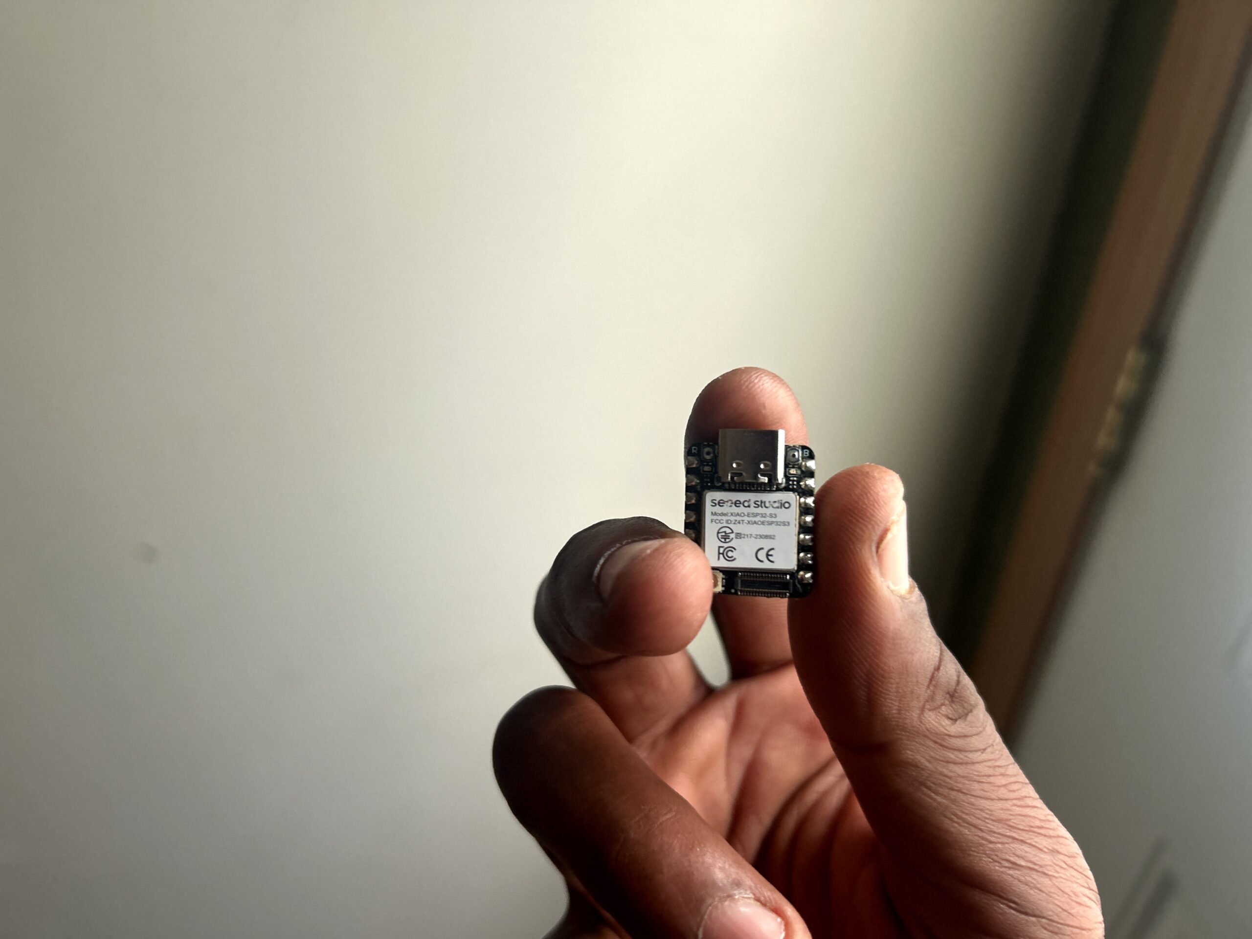
I found this awesome tutorial from Praetorian where they hacked a nicotine vape I broke open one of my vapes (I have tons more I can work with without breaking later) and found my pins I need to connect to but there was ONNNNNNNE tiny problem. I did not have a SWD probe/debugger but I did have a sh!t ton of ESP32 😂 so I started coding one.
SWD Protocol
The Pins
SWD drops the pin count significantly by utilizing a bi-directional data line. It requires only two mandatory pins for operation:
- SWDIO (Serial Wire Data Input/Output): A bi-directional line used to transfer commands and data between the host debugger (like a J-Link, ST-Link, or CMSIS-DAP probe) and the target microcontroller.
- SWCLK (Serial Wire Clock): A clock signal driven by the host debugger to synchronize data transfers.
In practical implementations, you will also typically route:
RESET: An optional pin to force a hardware reset on the target during connection or firmware flashing.
GND: A common ground reference essential for signal integrity.
VCC / VRef: To sense the target’s operating voltage so the debugger can match logic levels.
SWO (Serial Wire Output): An optional third pin used for single-wire tracing. It enables real-time logging and profiling without stopping execution or consuming a standard UART peripheral.
Knowing this I created a C++ Platformio program that consists of three files: main.cpp and swd.cpp and swd.h let’s dive into them one at a time.
Main.cpp
#include <Arduino.h>
#include "swd.h"

static SWD  swd;
static bool connected = false;

// ── helpers ───────────────────────────────────────────────────────────────────

static bool parseU32(const char *s, uint32_t *out) {
    char *end;
    unsigned long v = strtoul(s, &end, 0);
    if (end == s) return false;
    *out = (uint32_t)v;
    return true;
}

// ── command handlers ──────────────────────────────────────────────────────────

static void cmdConnect() {
    Serial.println("Connecting...");
    if (!swd.connect()) {
        Serial.println("FAIL — check SWDCLK/SWDIO wiring and target power");
        connected = false;
        return;
    }
    uint32_t id = 0;
    swd.dpRead(DP_IDCODE, &id);
    uint8_t  version  = (id >> 28) & 0xF;
    uint16_t partno   = (id >> 12) & 0xFFFF;
    uint16_t designer = (id >>  1) & 0x7FF;
    Serial.printf("IDCODE   : 0x%08X\n", id);
    Serial.printf("  Version : %u\n", version);
    Serial.printf("  Part    : 0x%03X\n", partno);
    Serial.printf("  Designer: 0x%03X%s\n", designer,
                  (designer == 0x23B) ? "  (ARM Ltd)" : "");
    Serial.println("Connected.");
    connected = true;
}

static void cmdIDCODE() {
    if (!connected) { Serial.println("Not connected"); return; }
    uint32_t id = 0;
    if (!swd.dpRead(DP_IDCODE, &id)) { Serial.println("FAIL"); return; }
    Serial.printf("IDCODE: 0x%08X\n", id);
}

static void cmdHalt() {
    if (!connected) { Serial.println("Not connected"); return; }
    if (!swd.halt())    { Serial.println("FAIL: halt"); return; }
    delay(10);
    if (swd.isHalted()) {
        uint32_t pc = 0;
        swd.readCoreReg(15, &pc);
        Serial.printf("Halted. PC = 0x%08X\n", pc);
    } else {
        Serial.println("Halt sent (target may not have stopped yet)");
    }
}

static void cmdResume() {
    if (!connected) { Serial.println("Not connected"); return; }
    if (!swd.resume()) { Serial.println("FAIL: resume"); return; }
    Serial.println("Running.");
}

static void cmdStep() {
    if (!connected) { Serial.println("Not connected"); return; }
    if (!swd.isHalted()) { Serial.println("Target must be halted first"); return; }
    if (!swd.step()) { Serial.println("FAIL: step"); return; }
    delay(2);
    uint32_t pc = 0;
    swd.readCoreReg(15, &pc);
    Serial.printf("Step. PC = 0x%08X\n", pc);
}

static void cmdReset() {
    if (!connected) { Serial.println("Not connected"); return; }
    swd.sysReset();
    delay(150);
    // Re-init DAP after system reset
    connected = swd.connect();
    Serial.println(connected ? "Reset OK. Reconnected." : "FAIL: reconnect after reset");
}

static void cmdRead(const char *args) {
    if (!connected) { Serial.println("Not connected"); return; }
    uint32_t addr;
    if (!parseU32(args, &addr)) { Serial.println("Usage: read <addr>"); return; }
    uint32_t val = 0;
    if (!swd.memRead32(addr, &val)) { Serial.println("FAIL: read error"); return; }
    Serial.printf("[0x%08X] = 0x%08X\n", addr, val);
}

static void cmdWrite(const char *args) {
    if (!connected) { Serial.println("Not connected"); return; }
    char a[20] = {}, b[20] = {};
    if (sscanf(args, "%19s %19s", a, b) != 2) {
        Serial.println("Usage: write <addr> <value>"); return;
    }
    uint32_t addr, val;
    if (!parseU32(a, &addr) || !parseU32(b, &val)) {
        Serial.println("Bad arguments"); return;
    }
    if (!swd.memWrite32(addr, val)) { Serial.println("FAIL: write error"); return; }
    Serial.printf("[0x%08X] <= 0x%08X  OK\n", addr, val);
}

static void cmdDump(const char *args) {
    if (!connected) { Serial.println("Not connected"); return; }
    char a[20] = {}, b[20] = {};
    uint32_t addr, count = 16;
    int n = sscanf(args, "%19s %19s", a, b);
    if (n < 1 || !parseU32(a, &addr)) {
        Serial.println("Usage: dump <addr> [words]"); return;
    }
    if (n >= 2) parseU32(b, &count);
    if (count > 256) count = 256;

    for (uint32_t i = 0; i < count; i++) {
        if (i % 4 == 0) Serial.printf("\n0x%08X:", addr + i * 4);
        uint32_t val = 0;
        if (!swd.memRead32(addr + i * 4, &val)) { Serial.println("  ERR"); return; }
        Serial.printf("  %08X", val);
    }
    Serial.println();
}

static const char *REG_NAMES[] = {
    "R0", "R1", "R2",  "R3",  "R4",  "R5",  "R6", "R7",
    "R8", "R9", "R10", "R11", "R12", "SP",  "LR", "PC", "xPSR"
};

static void cmdRegs() {
    if (!connected) { Serial.println("Not connected"); return; }
    if (!swd.isHalted()) { Serial.println("Target must be halted. Use 'halt' first."); return; }
    for (int i = 0; i <= 16; i++) {
        uint32_t val = 0;
        if (swd.readCoreReg(i, &val))
            Serial.printf("  %-5s : 0x%08X\n", REG_NAMES[i], val);
        else
            Serial.printf("  %-5s : ERROR\n", REG_NAMES[i]);
    }
}

static void cmdStatus() {
    if (!connected) { Serial.println("Not connected"); return; }
    uint32_t dhcsr = 0;
    if (!swd.memRead32(DHCSR, &dhcsr)) { Serial.println("FAIL"); return; }
    Serial.printf("DHCSR = 0x%08X — %s\n", dhcsr,
                  (dhcsr & DHCSR_S_HALT) ? "HALTED" : "RUNNING");
}

static void cmdClear() {
    swd.clearErrors();
    Serial.println("SWD error flags cleared.");
}

static void cmdResetPin(const char *args) {
    if (!*args) {
        uint8_t p = swd.getResetPin();
        if (p == SWD_NO_PIN) Serial.println("nRESET pin: not set");
        else                 Serial.printf("nRESET pin: GPIO%d\n", p);
        return;
    }
    uint32_t pin;
    if (!parseU32(args, &pin)) { Serial.println("Usage: resetpin <gpio>  (or 'none')"); return; }
    swd.setResetPin((uint8_t)pin);
    Serial.printf("nRESET → GPIO%u\n", pin);
}

static void cmdNReset() {
    if (swd.getResetPin() == SWD_NO_PIN) {
        Serial.println("No nRESET pin configured. Use: resetpin <gpio>");
        return;
    }
    Serial.println("Asserting nRESET...");
    swd.assertReset();
    delay(50);
    swd.releaseReset();
    delay(150);
    Serial.println("Released. Reconnecting...");
    connected = swd.connect();
    Serial.println(connected ? "Reconnected." : "FAIL: reconnect after reset");
}

static void cmdConnectHalt() {
    if (swd.getResetPin() == SWD_NO_PIN) {
        Serial.println("Requires nRESET pin. Use: resetpin <gpio>");
        return;
    }
    Serial.println("Connecting under reset...");
    if (!swd.connectHalt()) {
        Serial.println("FAIL — check wiring and target power");
        connected = false;
        return;
    }
    connected = true;
    uint32_t pc = 0;
    swd.readCoreReg(15, &pc);
    Serial.printf("Halted at reset vector. PC = 0x%08X\n", pc);
}

// GPIO pins exposed on the XIAO ESP32-S3 headers
static const uint8_t SCAN_PINS[]  = { 1, 2, 3, 4, 5, 6, 7, 8, 9, 43, 44 };
static const uint8_t SCAN_NPIN    = sizeof(SCAN_PINS);

static void cmdPinset(const char *args) {
    char a[8] = {}, b[8] = {};
    if (sscanf(args, "%7s %7s", a, b) != 2) {
        Serial.println("Usage: pinset <clk_gpio> <io_gpio>");
        Serial.printf("Current: SWDCLK=GPIO%d  SWDIO=GPIO%d\n",
                      swd.getCLKPin(), swd.getIOPin());
        return;
    }
    uint32_t clk, io;
    if (!parseU32(a, &clk) || !parseU32(b, &io)) {
        Serial.println("Bad pin numbers"); return;
    }
    swd.setPins((uint8_t)io, (uint8_t)clk);
    connected = false;
    Serial.printf("Pins set: SWDCLK=GPIO%u  SWDIO=GPIO%u\n", clk, io);
    Serial.println("Run 'connect' to try the new pins.");
}

// Try every CLK/IO pair from SCAN_PINS until we get a valid IDCODE.
static void cmdScan() {
    Serial.println("Scanning all GPIO pairs for SWD target...");
    Serial.println("(this takes ~30 s — the vape must be powered)");
    connected = false;

    for (uint8_t ci = 0; ci < SCAN_NPIN; ci++) {
        for (uint8_t ii = 0; ii < SCAN_NPIN; ii++) {
            if (ci == ii) continue;
            uint8_t clk = SCAN_PINS[ci];
            uint8_t io  = SCAN_PINS[ii];
            Serial.printf("  CLK=GPIO%-2d  IO=GPIO%-2d ... ", clk, io);

            swd.setPins(io, clk);
            uint32_t id = swd.probe();
            if (id) {
                Serial.printf("FOUND!  IDCODE=0x%08X\n", id);
                Serial.printf("Run: pinset %d %d\n", clk, io);
                Serial.println("Then: connect");
                return;
            }
            Serial.println("--");
        }
    }
    Serial.println("No SWD target found on any pair.");
    Serial.println("Check: target powered? GND shared? correct USB-C pins?");
    // Restore defaults
    swd.setPins(SWD_DEFAULT_IO, SWD_DEFAULT_CLK);
}

static void printHelp() {
    Serial.println(
        "\nConnection:\n"
        "  connect              line reset → IDCODE → power up → MEM-AP\n"
        "  connecthalt          connect under nRESET, halt at first instruction\n"
        "  scan                 sweep all GPIO pairs to find a live SWD target\n"
        "  pinset <clk> <io>    reassign SWDCLK / SWDIO GPIOs at runtime\n"
        "  resetpin [gpio]      set nRESET GPIO (show current if no arg)\n"
        "\nExecution:\n"
        "  halt                 halt the CPU\n"
        "  resume               resume execution\n"
        "  step                 single-step one instruction (must be halted)\n"
        "  nreset               pulse nRESET low then reconnect\n"
        "  reset                software reset via AIRCR SYSRESETREQ\n"
        "  status               show DHCSR — running or halted\n"
        "\nInspection:\n"
        "  regs                 dump R0-R15, xPSR  (must be halted)\n"
        "  idcode               re-read raw IDCODE\n"
        "  read  <addr>         read one 32-bit word\n"
        "  write <addr> <val>   write one 32-bit word\n"
        "  dump  <addr> [n]     hex dump n words (default 16, max 256)\n"
        "  clear                clear SWD sticky error flags (ABORT)\n"
        "\nDefault pins (XIAO ESP32-S3):\n"
        "  SWDCLK → D8 / GPIO7\n"
        "  SWDIO  → D9 / GPIO8\n"
        "  nRESET → not set    (use 'resetpin <gpio>' to assign)\n"
    );
}

// ── command dispatcher ────────────────────────────────────────────────────────

static void dispatch(char *line) {
    while (*line == ' ') line++;
    if (!*line) return;

    char *cmd = line;
    char *args = line;
    while (*args && *args != ' ') args++;
    if (*args) { *args++ = '\0'; }
    while (*args == ' ') args++;

    if      (!strcmp(cmd, "connect")) cmdConnect();
    else if (!strcmp(cmd, "idcode"))  cmdIDCODE();
    else if (!strcmp(cmd, "halt"))    cmdHalt();
    else if (!strcmp(cmd, "resume"))  cmdResume();
    else if (!strcmp(cmd, "step"))    cmdStep();
    else if (!strcmp(cmd, "reset"))   cmdReset();
    else if (!strcmp(cmd, "status"))  cmdStatus();
    else if (!strcmp(cmd, "regs"))    cmdRegs();
    else if (!strcmp(cmd, "read"))    cmdRead(args);
    else if (!strcmp(cmd, "write"))   cmdWrite(args);
    else if (!strcmp(cmd, "dump"))    cmdDump(args);
    else if (!strcmp(cmd, "clear"))        cmdClear();
    else if (!strcmp(cmd, "pinset"))       cmdPinset(args);
    else if (!strcmp(cmd, "scan"))         cmdScan();
    else if (!strcmp(cmd, "resetpin"))     cmdResetPin(args);
    else if (!strcmp(cmd, "nreset"))       cmdNReset();
    else if (!strcmp(cmd, "connecthalt"))  cmdConnectHalt();
    else if (!strcmp(cmd, "help"))         printHelp();
    else Serial.printf("Unknown: '%s'  (type 'help')\n", cmd);

    Serial.print("> ");
}

// ── Arduino entry points ──────────────────────────────────────────────────────

static char   lineBuf[128];
static uint8_t lineLen = 0;

void setup() {
    Serial.begin(115200);
    // USB CDC: wait for the host to open the port (up to ~5 s), then greet.
    // Without this the banner gets sent before the terminal is ready.
    uint32_t t = millis();
    while (!Serial && (millis() - t < 5000)) delay(10);
    Serial.println("\n=== ESP32-S3 SWD Debugger ===");
    printHelp();
    Serial.print("\n> ");
}

void loop() {
    while (Serial.available()) {
        char c = (char)Serial.read();
        if (c == '\r') continue;
        if (c == '\n') {
            lineBuf[lineLen] = '\0';
            Serial.println();
            dispatch(lineBuf);
            lineLen = 0;
        } else if (c == '\b' || c == 127) {
            if (lineLen > 0) { lineLen--; Serial.print("\b \b"); }
        } else if (lineLen < sizeof(lineBuf) - 1) {
            lineBuf[lineLen++] = c;
            Serial.print(c);
        }
    }
}
1. The Terminal Engine and Dispatcher
The firmware relies on standard Arduino entry points to drive a non-blocking character parser. Inside setup(), the code initializes the hardware serial interface at 115200 baud and loops until an active USB CDC connection is established, preventing the initial banner from dropping before a terminal viewer opens.
The main loop() continuously monitors Serial.available(). It streams incoming characters into a raw character buffer (lineBuf), tracks length limits to prevent buffer overflows, and safely handles backspaces (\b or ASCII 127) by dropping the buffer index and echoing terminal erasure commands (\b \b).
When a newline character (\n) is intercepted, the engine seals the string with a null terminator (\0) and forwards it to the dispatch() routing function. The dispatcher strips leading whitespace, tokenizes the raw text into distinct command and argument pointers by searching for space boundaries, and matches the command string via strcmp to its respective execution handler.
2. Low-Level SWD Discovery and Connection
Target acquisition is managed by cmdConnect() and cmdScan(). When the connect command is issued, swd.connect() triggers a low-level line reset sequence (driving SWDIO high for more than 50 clock cycles) to wake up the target’s Debug Port (DP). If successful, it reads the raw 32-bit DP_IDCODE from the target using swd.dpRead().
The firmware then executes bitwise shifts and masking operations to extract and print the silicon’s metadata:
version: Isolated by shifting 28 bits right and applying a0xFmask.partno: Isolated by shifting 12 bits right and applying a0xFFFFmask.designer: Isolated by shifting 1 bit right and applying a0x7FFmask (checking if it matches ARM Ltd’s JEDEC identity code0x23B).
If the exact pinout of the target board is unknown, cmdScan() implements a automated hardware prober. It runs nested loops across a predefined array of physical GPIO headers (SCAN_PINS), dynamically reassigning clock (SWDCLK) and data (SWDIO) lines via swd.setPins() before firing a low-overhead swd.probe() request. If a valid IDCODE drops out of the sweep, the firmware breaks execution and outputs the precise pin parameters required to establish a stable link.
3. Execution Control and Memory Architecture
Once connected evaluates to true, the firmware can directly mutate target execution and state through the processor’s Debug Halting Control and Status Register (DHCSR). Calling cmdHalt() updates the debug registers to pause the CPU core. Once halted, it calls swd.readCoreReg(15, &pc) to query core register 15—the Program Counter (PC)—revealing exactly where execution froze. Similarly, cmdStep() advances the target by a single assembly instruction before instantly re-reading the updated Program Counter.
For direct physical memory access, commands like read, write, and dump wrap character inputs into numerical values using parseU32 (a thin wrapper around strtoul). These handlers route transactions directly through the target’s internal bus via the Memory Access Port (MEM-AP).
cmdRead()andcmdWrite()invokeswd.memRead32()andswd.memWrite32()respectively to read or write individual 32-bit words at explicit memory addresses.cmdDump()loops through consecutive 32-bit words up to a hard cap of 256, formatting the data into a structured hex grid over the serial console to allow rapid analysis of RAM arrays, flash boundaries, or peripheral registers at runtime.
swd.h
#pragma once
#include <Arduino.h>

// ACK values
#define SWD_ACK_OK     0x01
#define SWD_ACK_WAIT   0x02
#define SWD_ACK_FAULT  0x04
#define SWD_ACK_ERROR  0xFF  // parity mismatch or comms failure

// DP register addresses (word-aligned, bits [3:2] used in packet)
#define DP_IDCODE    0x00  // R
#define DP_ABORT     0x00  // W
#define DP_CTRLSTAT  0x04
#define DP_SELECT    0x08
#define DP_RDBUFF    0x0C

// CTRL/STAT bits
#define CTRL_CSYSPWRUPACK  (1UL << 31)
#define CTRL_CSYSPWRUPREQ  (1UL << 30)
#define CTRL_CDBGPWRUPACK  (1UL << 29)
#define CTRL_CDBGPWRUPREQ  (1UL << 28)
#define CTRL_STICKYERR     (1UL << 5)
#define CTRL_STICKYORUN    (1UL << 1)

// MEM-AP register offsets (bank 0)
#define AP_CSW  0x00
#define AP_TAR  0x04
#define AP_DRW  0x0C

// CSW value: DbgSwEnable off (set by HW), privileged, word, single-increment
#define AP_CSW_VALUE  0x23000052UL

// Cortex-M debug register addresses
#define DHCSR  0xE000EDF0UL  // Debug Halting Control & Status
#define DCRSR  0xE000EDF4UL  // Debug Core Register Selector
#define DCRDR  0xE000EDF8UL  // Debug Core Register Data
#define DEMCR  0xE000EDFCUL  // Debug Exception & Monitor Control
#define AIRCR  0xE000ED0CUL  // Application Interrupt & Reset Control

// DHCSR bits
#define DHCSR_DBGKEY     0xA05F0000UL
#define DHCSR_C_DEBUGEN  (1UL << 0)
#define DHCSR_C_HALT     (1UL << 1)
#define DHCSR_C_STEP     (1UL << 2)
#define DHCSR_C_MASKINTS (1UL << 3)
#define DHCSR_S_REGRDY   (1UL << 16)
#define DHCSR_S_HALT     (1UL << 17)

// DEMCR bits
#define DEMCR_TRCENA        (1UL << 24)
#define DEMCR_VC_CORERESET  (1UL << 0)   // halt on reset vector

// Sentinel meaning "no pin assigned"
#define SWD_NO_PIN  0xFF

// Default pins for XIAO ESP32-S3
#define SWD_DEFAULT_CLK  7   // D8 / GPIO7
#define SWD_DEFAULT_IO   8   // D9 / GPIO8

class SWD {
public:
    SWD(uint8_t swdio = SWD_DEFAULT_IO, uint8_t swdclk = SWD_DEFAULT_CLK);

    // Reconfigure SWD pins at runtime (releases old pins first)
    void setPins(uint8_t swdio, uint8_t swdclk);
    uint8_t getIOPin()  const { return _io;  }
    uint8_t getCLKPin() const { return _clk; }

    // Optional nRESET line (open-drain, active-low). Pass SWD_NO_PIN to disable.
    void setResetPin(uint8_t pin);
    uint8_t getResetPin() const { return _rst; }
    void assertReset();   // drive nRESET LOW
    void releaseReset();  // float nRESET (let pull-up take it HIGH)

    // Full connection sequence: line reset → IDCODE check → power up → MEM-AP
    bool connect();

    // Connect under reset: assert nRESET, init DAP, arm vector-catch, release.
    // Target halts at the very first instruction after reset. Requires nRESET pin.
    bool connectHalt();

    // Probe-only connect: returns IDCODE if SWD link is found, 0 on failure.
    // Does NOT power up or set up MEM-AP — use connect() for full init.
    uint32_t probe();

    // DP-level access
    bool dpRead(uint8_t addr, uint32_t *out);
    bool dpWrite(uint8_t addr, uint32_t val);

    // AP-level access (handles SELECT automatically)
    bool apRead(uint8_t ap, uint8_t reg, uint32_t *out);
    bool apWrite(uint8_t ap, uint8_t reg, uint32_t val);

    // Memory access via MEM-AP 0
    bool memRead32(uint32_t addr, uint32_t *out);
    bool memWrite32(uint32_t addr, uint32_t val);
    bool memRead(uint32_t addr, uint32_t *buf, size_t nWords);

    // Cortex-M debug operations (target must be connected + powered)
    bool halt();
    bool resume();
    bool step();
    bool sysReset();
    bool isHalted();

    // Core register access (target must be halted)
    bool readCoreReg(uint8_t reg, uint32_t *out);
    bool writeCoreReg(uint8_t reg, uint32_t val);

    // Clear sticky error flags in DP ABORT
    void clearErrors();

private:
    uint8_t _io, _clk;
    uint8_t _rst;              // nRESET pin, SWD_NO_PIN if unused
    uint8_t _selAP, _selBank;  // cached SELECT state

    void ioOut();
    void ioIn();
    void writeBit(uint8_t b);
    uint8_t readBit();
    void clkPulse();

    void lineReset();
    void jtagToSWD();
    void idleCycles(uint8_t n);

    uint8_t buildReq(bool ap, bool rd, uint8_t reg);
    uint8_t xfer(bool ap, bool rd, uint8_t reg, uint32_t *data);

    bool selectAP(uint8_t ap, uint8_t bank);
    bool powerUp();
    bool setupMEMAP();
};
1. Protocol Tokens and Register Footprints
The top half of the header uses standard preprocessor directives (#define) to build a rigid dictionary of the ARM architecture’s hardware requirements. The first block establishes the specific response bytes the target can return during a transaction turnaround, such as SWD_ACK_OK or SWD_ACK_WAIT.
Following this are the hardcoded addresses for both the Debug Port (DP) and Access Port (AP) registers:
- DP Registers:
DP_IDCODEreads device identification, whileDP_SELECThandles routing between different internal Access Ports and register banks. - AP Registers: Low-level memory bus operations route through the Memory Access Port using
AP_CSW(Control Status Word),AP_TAR(Transfer Address Register), andAP_DRW(Data Read/Write). The specific bitmaskAP_CSW_VALUEinstructs the target to execute memory accesses as clean 32-bit words with automatic address incrementing turned on. - Cortex-M Debug Registers: The final macro block maps the memory locations for the Core Debug registers located at the top of the processor’s system space (the
0xE000EDF0block). This includesDHCSR, which forces the CPU to halt or single-step, andDEMCR, which allows the host to trap the processor at its very first boot instruction using vector catching (DEMCR_VC_CORERESET).
2. The Public High-Level API
The public block of the SWD class exposes a clean interface for application-level code to interrogate a target device without needing to understand raw bit arrangements. The lifecycle begins with initialization, where the constructor assigns the default clock and data pins (configured here for the Seeed Studio XIAO ESP32-S3’s hardware map), while setPins() and setResetPin() manage physical wire reassignments at runtime. Physical reset control is exposed through open-drain abstractions (assertReset and releaseReset) to cleanly float or pull down the target’s physical nRESET line.
Connection management is divided into three functional paradigms:
probe()acts as a fast, low-overhead link verifier that checks for anIDCODEwithout modifying system state.connect()executes the full operational sequence required to power up the internal debug domains and latch onto the core.connectHalt()implements a specialized sequence that pins the hardware reset line, arms a vector catch, and releases the reset to catch the processor before any firmware can execute.
Once an active connection is established, developers are provided with high-level functions like halt(), resume(), step(), and register access blocks (readCoreReg/writeCoreReg). These are backed by automated memory methods like memRead32() and memWrite32(), which let you read and write data across the target’s entire internal memory map through a single call.
3. The Private Bit-Banging Engine
The private partition contains the raw, low-overhead state tracking and driver primitives needed to translate high-level commands into physical voltage fluctuations on the wire. The integer variables _selAP and _selBank act as a local software cache. By remembering which Access Port and register bank the host is currently talking to, the code avoids sending redundant DP_SELECT write packets over the wire, optimizing data throughput during massive memory dumps.
The lower methods handle wire-level operations:
ioOut()andioIn()rapidly reconfigure the microcontroller’s sharedSWDIOdata pin between input and output modes.writeBit(),readBit(), andclkPulse()form the basic clock-synchronized IO foundation.lineReset()andjtagToSWD()output the exact bitstream signatures (such as driving the data line high for 50+ cycles followed by a specific 16-bit switching key) required to reset the wire state machine and kick the target out of JTAG mode into SWD mode.buildReq()andxfer()assemble the mandatory 8-bit request frame (comprising start bits, AP/DP selectors, read/write flags, address bits, and parity), transmit the command, handle the wire turnaround phase, and verify incoming target acknowledgements and data parity bits.
swd.cpp
#include "swd.h"

// Half-period in µs → clock frequency ≈ 1/(2*HALF_US) Hz
// 1 µs → ~500 kHz; safe for most Cortex-M targets
#define HALF_US 1

SWD::SWD(uint8_t swdio, uint8_t swdclk)
    : _io(swdio), _clk(swdclk), _rst(SWD_NO_PIN),
      _selAP(0xFF), _selBank(0xFF) {}

void SWD::setPins(uint8_t swdio, uint8_t swdclk) {
    pinMode(_io,  INPUT);
    pinMode(_clk, INPUT);
    _io      = swdio;
    _clk     = swdclk;
    _selAP   = 0xFF;
    _selBank = 0xFF;
}

void SWD::setResetPin(uint8_t pin) {
    if (_rst != SWD_NO_PIN) pinMode(_rst, INPUT);  // release old pin
    _rst = pin;
    if (_rst != SWD_NO_PIN) pinMode(_rst, INPUT);  // start released (hi-Z)
}

// nRESET is open-drain active-low: drive LOW to assert, hi-Z to release.
void SWD::assertReset() {
    if (_rst == SWD_NO_PIN) return;
    pinMode(_rst, OUTPUT);
    digitalWrite(_rst, LOW);
}

void SWD::releaseReset() {
    if (_rst == SWD_NO_PIN) return;
    pinMode(_rst, INPUT);  // let the target's pull-up take it HIGH
}

// ── pin helpers ──────────────────────────────────────────────────────────────

void SWD::ioOut() { pinMode(_io, OUTPUT); }
void SWD::ioIn()  { pinMode(_io, INPUT);  }

// Clock starts LOW. Data is driven before clock rises; sampled at rising edge.
void SWD::writeBit(uint8_t b) {
    digitalWrite(_io, b & 1);
    delayMicroseconds(HALF_US);
    digitalWrite(_clk, HIGH);
    delayMicroseconds(HALF_US);
    digitalWrite(_clk, LOW);
}

uint8_t SWD::readBit() {
    delayMicroseconds(HALF_US);
    digitalWrite(_clk, HIGH);
    uint8_t b = digitalRead(_io);  // sample at rising edge
    delayMicroseconds(HALF_US);
    digitalWrite(_clk, LOW);
    return b;
}

void SWD::clkPulse() {
    delayMicroseconds(HALF_US);
    digitalWrite(_clk, HIGH);
    delayMicroseconds(HALF_US);
    digitalWrite(_clk, LOW);
}

// ── line-level sequences ─────────────────────────────────────────────────────

void SWD::lineReset() {
    ioOut();
    digitalWrite(_io, HIGH);
    for (int i = 0; i < 56; i++) clkPulse();
}

// Switch from JTAG to SWD: send 0xE79E as 16 bits, LSB first
void SWD::jtagToSWD() {
    ioOut();
    uint16_t seq = 0xE79E;
    for (int i = 0; i < 16; i++) writeBit((seq >> i) & 1);
}

void SWD::idleCycles(uint8_t n) {
    ioOut();
    digitalWrite(_io, LOW);
    for (uint8_t i = 0; i < n; i++) clkPulse();
}

// ── SWD packet transfer ───────────────────────────────────────────────────────

// Build the 8-bit request header (Start|APnDP|RnW|A[2]|A[3]|Parity|Stop|Park)
uint8_t SWD::buildReq(bool ap, bool rd, uint8_t reg) {
    uint8_t A2  = (reg >> 2) & 1;
    uint8_t A3  = (reg >> 3) & 1;
    uint8_t par = (uint8_t)ap ^ (uint8_t)rd ^ A2 ^ A3;
    return (1        )       // Start
         | ((uint8_t)ap << 1) // APnDP
         | ((uint8_t)rd << 2) // RnW
         | (A2 << 3)          // A[2]
         | (A3 << 4)          // A[3]
         | (par << 5)         // Parity
         | (0  << 6)          // Stop
         | (1  << 7);         // Park
}

// Single SWD packet. Returns SWD_ACK_* constant.
// For writes, *data must point to the value to write.
// For reads, *data is filled with the received value on SWD_ACK_OK.
uint8_t SWD::xfer(bool ap, bool rd, uint8_t reg, uint32_t *data) {
    // ── request phase (host drives) ──────────────────────────────────────────
    uint8_t req = buildReq(ap, rd, reg);
    ioOut();
    for (int i = 0; i < 8; i++) writeBit((req >> i) & 1);

    // ── turnaround: host releases SWDIO ─────────────────────────────────────
    ioIn();
    clkPulse();

    // ── ACK (3 bits, target drives) ─────────────────────────────────────────
    uint8_t ack = 0;
    for (int i = 0; i < 3; i++) ack |= (readBit() << i);

    if (rd) {
        // ── READ: target continues to drive data ─────────────────────────────
        if (ack == SWD_ACK_OK) {
            uint32_t val = 0;
            uint8_t  par = 0;
            for (int i = 0; i < 32; i++) {
                uint8_t b = readBit();
                val |= ((uint32_t)b << i);
                par ^= b;
            }
            uint8_t rxPar = readBit();

            // turnaround: target releases, host takes over
            ioOut();
            clkPulse();

            if (data) *data = val;
            return (par == rxPar) ? SWD_ACK_OK : SWD_ACK_ERROR;
        } else {
            // WAIT or FAULT: turnaround then idle
            ioOut();
            clkPulse();
            idleCycles(8);
            return ack;
        }
    } else {
        // ── WRITE: turnaround, then host drives data ──────────────────────────
        ioOut();
        clkPulse();  // turnaround

        if (ack == SWD_ACK_OK && data) {
            uint8_t par = 0;
            for (int i = 0; i < 32; i++) {
                uint8_t b = (*data >> i) & 1;
                writeBit(b);
                par ^= b;
            }
            writeBit(par);
        }
        idleCycles(2);  // capture / idle
        return ack;
    }
}

// ── DP access (with WAIT retry) ───────────────────────────────────────────────

bool SWD::dpRead(uint8_t addr, uint32_t *out) {
    for (int r = 0; r < 8; r++) {
        uint8_t ack = xfer(false, true, addr, out);
        if (ack == SWD_ACK_OK)   return true;
        if (ack != SWD_ACK_WAIT) return false;
    }
    return false;
}

bool SWD::dpWrite(uint8_t addr, uint32_t val) {
    for (int r = 0; r < 8; r++) {
        uint8_t ack = xfer(false, false, addr, &val);
        if (ack == SWD_ACK_OK)   return true;
        if (ack != SWD_ACK_WAIT) return false;
    }
    return false;
}

// ── AP SELECT helper ──────────────────────────────────────────────────────────

bool SWD::selectAP(uint8_t ap, uint8_t bank) {
    if (_selAP == ap && _selBank == bank) return true;
    uint32_t sel = ((uint32_t)ap << 24) | ((uint32_t)bank << 4);
    if (!dpWrite(DP_SELECT, sel)) return false;
    _selAP   = ap;
    _selBank = bank;
    return true;
}

// ── AP access ────────────────────────────────────────────────────────────────
// AP reads are "posted": the xfer initiates the read and the result comes
// back via DP RDBUFF (or the next AP read). We always use RDBUFF here.

bool SWD::apRead(uint8_t ap, uint8_t reg, uint32_t *out) {
    uint8_t bank = (reg >> 4) & 0xF;
    if (!selectAP(ap, bank)) return false;

    uint32_t dummy = 0;
    for (int r = 0; r < 8; r++) {
        uint8_t ack = xfer(true, true, reg & 0x0F, &dummy);
        if (ack == SWD_ACK_OK)   break;
        if (ack != SWD_ACK_WAIT) return false;
    }
    return dpRead(DP_RDBUFF, out);
}

bool SWD::apWrite(uint8_t ap, uint8_t reg, uint32_t val) {
    uint8_t bank = (reg >> 4) & 0xF;
    if (!selectAP(ap, bank)) return false;

    for (int r = 0; r < 8; r++) {
        uint8_t ack = xfer(true, false, reg & 0x0F, &val);
        if (ack == SWD_ACK_OK)   return true;
        if (ack != SWD_ACK_WAIT) return false;
    }
    return false;
}

// ── high-level init ───────────────────────────────────────────────────────────

bool SWD::powerUp() {
    if (!dpWrite(DP_CTRLSTAT, CTRL_CSYSPWRUPREQ | CTRL_CDBGPWRUPREQ)) return false;
    for (int i = 0; i < 100; i++) {
        uint32_t stat = 0;
        if (!dpRead(DP_CTRLSTAT, &stat)) return false;
        uint32_t ack_bits = CTRL_CSYSPWRUPACK | CTRL_CDBGPWRUPACK;
        if ((stat & ack_bits) == ack_bits) return true;
        delay(1);
    }
    return false;
}

bool SWD::setupMEMAP() {
    return apWrite(0, AP_CSW, AP_CSW_VALUE);
}

// probe(): line reset → JTAG-to-SWD → IDCODE read only.
// Returns IDCODE on success, 0 on failure. Leaves pins floating afterward.
uint32_t SWD::probe() {
    pinMode(_clk, OUTPUT);
    pinMode(_io,  OUTPUT);
    digitalWrite(_clk, LOW);
    digitalWrite(_io,  LOW);
    _selAP   = 0xFF;
    _selBank = 0xFF;

    lineReset();
    jtagToSWD();
    lineReset();
    idleCycles(2);

    uint32_t id = 0;
    if (dpRead(DP_IDCODE, &id) && id != 0 && id != 0xFFFFFFFF) return id;

    // Float pins so the next combination can be tried cleanly
    pinMode(_clk, INPUT);
    pinMode(_io,  INPUT);
    return 0;
}

bool SWD::connect() {
    pinMode(_clk, OUTPUT);
    pinMode(_io,  OUTPUT);
    digitalWrite(_clk, LOW);
    digitalWrite(_io,  LOW);

    _selAP   = 0xFF;
    _selBank = 0xFF;

    lineReset();
    jtagToSWD();
    lineReset();
    idleCycles(2);

    uint32_t id = 0;
    for (int r = 0; r < 3; r++) {
        if (dpRead(DP_IDCODE, &id) && id != 0 && id != 0xFFFFFFFF) goto got_id;
        lineReset();
        idleCycles(2);
    }
    return false;

got_id:
    if (!powerUp())    return false;
    if (!setupMEMAP()) return false;
    return true;
}

// Assert nRESET, connect the DAP while held in reset, arm vector-catch on the
// reset vector, then release. The CPU halts at its very first instruction.
// Returns false if nRESET pin is not configured or connection fails.
bool SWD::connectHalt() {
    if (_rst == SWD_NO_PIN) return false;

    assertReset();
    delay(10);

    if (!connect()) {
        releaseReset();
        return false;
    }

    // Arm vector-catch so the core halts at the reset vector
    if (!memWrite32(DEMCR, DEMCR_TRCENA | DEMCR_VC_CORERESET)) {
        releaseReset();
        return false;
    }

    // Pre-arm the halt flag so debug is enabled before reset exits
    memWrite32(DHCSR, DHCSR_DBGKEY | DHCSR_C_HALT | DHCSR_C_DEBUGEN);

    releaseReset();

    // Wait for the core to halt (it should be nearly instant)
    for (int i = 0; i < 200; i++) {
        if (isHalted()) return true;
        delay(2);
    }
    return false;
}

void SWD::clearErrors() {
    dpWrite(DP_ABORT, 0x1EUL);  // clear WDERR, STKERR, STKCMP, ORUNERR
    _selAP   = 0xFF;
    _selBank = 0xFF;
}

// ── memory access ─────────────────────────────────────────────────────────────

bool SWD::memRead32(uint32_t addr, uint32_t *out) {
    if (!apWrite(0, AP_TAR, addr)) return false;
    return apRead(0, AP_DRW, out);
}

bool SWD::memWrite32(uint32_t addr, uint32_t val) {
    if (!apWrite(0, AP_TAR, addr)) return false;
    return apWrite(0, AP_DRW, val);
}

bool SWD::memRead(uint32_t addr, uint32_t *buf, size_t nWords) {
    for (size_t i = 0; i < nWords; i++) {
        if (!memRead32(addr + i * 4, &buf[i])) return false;
    }
    return true;
}

// ── Cortex-M debug operations ─────────────────────────────────────────────────

bool SWD::halt() {
    return memWrite32(DHCSR, DHCSR_DBGKEY | DHCSR_C_HALT | DHCSR_C_DEBUGEN);
}

bool SWD::resume() {
    return memWrite32(DHCSR, DHCSR_DBGKEY | DHCSR_C_DEBUGEN);
}

bool SWD::step() {
    // Mask interrupts so the step doesn't fire an ISR
    return memWrite32(DHCSR, DHCSR_DBGKEY | DHCSR_C_STEP | DHCSR_C_MASKINTS | DHCSR_C_DEBUGEN);
}

bool SWD::isHalted() {
    uint32_t dhcsr = 0;
    return memRead32(DHCSR, &dhcsr) && (dhcsr & DHCSR_S_HALT);
}

bool SWD::sysReset() {
    // AIRCR: VECTKEY | SYSRESETREQ
    return memWrite32(AIRCR, 0x05FA0004UL);
}

bool SWD::readCoreReg(uint8_t reg, uint32_t *out) {
    if (!memWrite32(DCRSR, reg & 0x1F)) return false;
    uint32_t dhcsr = 0;
    for (int i = 0; i < 100; i++) {
        if (!memRead32(DHCSR, &dhcsr)) return false;
        if (dhcsr & DHCSR_S_REGRDY) return memRead32(DCRDR, out);
        delayMicroseconds(10);
    }
    return false;
}

bool SWD::writeCoreReg(uint8_t reg, uint32_t val) {
    if (!memWrite32(DCRDR, val))                            return false;
    if (!memWrite32(DCRSR, (1UL << 16) | (reg & 0x1F)))    return false;
    uint32_t dhcsr = 0;
    for (int i = 0; i < 100; i++) {
        if (!memRead32(DHCSR, &dhcsr)) return false;
        if (dhcsr & DHCSR_S_REGRDY)   return true;
        delayMicroseconds(10);
    }
    return false;
}
This implementation file translates the architectural framework of your header into concrete execution steps, managing everything from exact microsecond line timing up to core halting routines.
Here is a breakdown of how the source code executes its low-level hardware manipulation.
1. High-Performance Timing and Bit-Banging Primitives
At the lowest level, the driver establishes wire communication using manual pin toggling synchronized by the HALF_US macro. Set to 1 microsecond, this creates a clean half-period delay, yielding a stable ~500 kHz clock cycle that is safe for long lines and most ARM Cortex-M targets. The fundamental I/O primitives—writeBit(), readBit(), and clkPulse()—implement standard SPI-like synchronous signaling on top of the shared SWDIO pin.
Data is strictly driven onto the line before the clock rises, and sampled by the target on the rising edge of SWCLK. To transition between transmitting and receiving without causing a short circuit on the data line, the driver manipulates ioOut() and ioIn(). These call Arduino’s underlying pinMode() to seamlessly flip the SWDIO line between a low-impedance output and a high-impedance input.
2. Protocol Frame Assembly and Packet Handling
The transactional heart of the code lies within the xfer() method, which handles a complete, multi-phase SWD packet. It first invokes buildReq() to calculate parity over the target address and read/write flags, formatting an 8-bit command byte wrapped in explicit start, stop, and park bits.
Once the host streams this byte out, it relinquishes control of the line during a precise one-cycle “turnaround” phase, shifts into input mode, and reads a 3-bit acknowledgement frame (ack) driven back by the target. If the transaction is a read and returns SWD_ACK_OK, the host clocks in 32 data bits followed by a final parity bit, tracking cumulative parity on the fly via an exclusive-OR accumulator (par ^= b).
For writes, the sequence is inverted: the host clears the turnaround phase, assumes ownership of the data line, and streams out the payload along with its calculated parity before pushing trailing idle cycles to settle the target’s internal state machine. High-level wrappers dpRead() and dpWrite() wrap this machine in a loop that automatically retries transactions up to eight times if the target asserts a SWD_ACK_WAIT response, preventing transient bus collisions from breaking execution.
3. State Caching and Access Port Topography
To maximize throughput, the driver uses optimization shielding inside selectAP(). It maintains local copies of the current Access Port (_selAP) and register bank (_selBank) settings. If consecutive commands address the exact same register bank, the driver completely skips writing to the target’s DP_SELECT register, eliminating unnecessary overhead during consecutive transfers.
This mechanism is critical for apRead() and apWrite(). Because ARM Access Port reads are inherently “posted”—meaning a request initiated on the bus does not return its data until the subsequent transaction—apRead() fires the primary AP request, handles potential wait states, and then executes a follow-up read on the Debug Port’s read buffer (DP_RDBUFF) to extract the staged data.
4. Advanced Lifecycle and Core Debug Halting
The complex lifecycles of target discovery and control are finalized in connect(), connectHalt(), and core register manipulators. The standard connect() sequence wakes the target by firing a 56-cycle continuous high signal (lineReset()), sending the mandatory 16-bit JTAG-to-SWD switching key (0xE79E), executing a second line reset, and asserting a power-up request to the internal system and debug power domains via DP_CTRLSTAT.
The connectHalt() method goes an explicit step further to intercept execution on secured or crashing targets. It asserts a physical hardware reset by driving the target’s nRESET line low, hooks into the alive DAP, and writes to the Core Debug Exception and Monitor Control Register (DEMCR) to arm a vector catch (DEMCR_VC_CORERESET). It then primes the core’s halting state machine in DHCSR, releases the physical reset line, and monitors status flags until the processor halts directly at its first instruction vector before a single line of application firmware can run.
Finally, readCoreReg() and writeCoreReg() manipulate internal CPU registers (R0-R15) by using a dual-register handshake: the host writes the target register index to the Selector Register (DCRSR), polls DHCSR until the data-ready flag (DHCSR_S_REGRDY) resolves, and then reads or writes the actual payload through the Data Register (DCRDR).
This was fun!
After building my swd software I loaded it on my Seeed Studio XIAO ESP32-S3 Sense and immediately got to work on my RAZ board. I was able to probe and dump the firmware successfully. All of my source code is publicly available on Github. Follow me as I go into the new firmware I will put on my vapes. Leave a comment to let me know what you want to see run on the boards!